

1.1 Semiconductors
Semiconductors are materials whose electrical properties are intermediate between those of conductors, which offer little resistance to the flow of electric current, and insulators, which inhibit the flow of electricity. They are usually made from silicon, although as you’ll see PV cells can be made from other materials.
The silicon semiconductors used in photovoltaics are of two types: n-type (negative) and a p-type (positive)
N-type semiconductors are made from crystalline silicon that has been ‘doped’ with tiny quantities of an impurity, usually phosphorus, in such a way that the doped material possesses a surplus of free electrons. Because electrons possess a negative electrical charge, silicon doped in this way is known as an n-type semiconductor.
P-type semiconductors are doped with very small amounts of a different impurity, usually boron, which causes the material to have a deficit of free electrons. These missing electrons are called ‘holes’. Because the absence of a negatively charged electron can be considered equivalent to a positively charged particle, silicon doped in this way is known as a p-type semiconductor.
P–n junctions
A p–n junction is created by joining these dissimilar Negative (n) and Positive (p) semiconductors. This sets up an electric field in the region of the junction, which causes negatively charged particles to move in one direction and positively charged particles to move in the opposite direction.
Light can be considered to consist of a stream of tiny particles of energy, called photons. When photons from light of a suitable wavelength fall within a p–n junction, they can transfer their energy to some of the electrons in the material, so ‘promoting’ them to a higher energy level.
Normally, these electrons help to hold the material together by forming so-called ‘valence’ bonds with adjoining atoms, and in this ‘valence band’ they cannot move. But in their new ‘excited’ state, these electrons have been raised to an energy level known as the ‘conduction band’ and become free to conduct electric current by moving through the material. The difference in energy between the ‘valence’ band and the conduction band is known as the band gap.
The essential principles underlying the operation of a silicon solar cell are described in Box 1 below, Figure 2
Box 1: The essential principles underlying the operation of a silicon solar cell
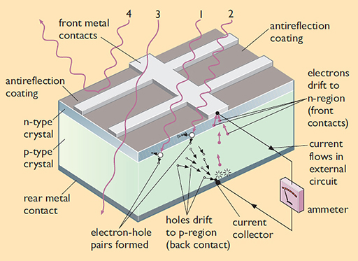
The silicon solar cell shown in Figure 2 above is a wafer of p-type silicon with a thin layer of n-type silicon on one side. When a photon of light with the appropriate amount of energy penetrates the cell near the junction of the two types of crystal and encounters a silicon atom (1), it dislodges one of the electrons, which leaves behind a hole.
The electron tends to migrate up into the layer of n-type silicon and the hole tends to migrate down into the layer of p-type silicon. The electron then travels to a metallic current collector on the front surface of the cell, generates an electric current in the external circuit and then re-emerges in the layer of p-type silicon, where it can recombine with waiting holes.
If a photon with an amount of energy greater than the band gap strikes a silicon atom (2), it again gives rise to an electron–hole pair, and the excess energy is converted into heat. A photon with an amount of energy smaller than the band gap will pass right through the cell (3), so that it gives up virtually no energy along the way.
Some photons are reflected from the front surface of the cell even when it has an antireflection coating (4). Still other photons are lost because they are blocked from reaching the crystal by the current collectors that cover part of the front surface.
(Source for all above text and figure: adapted from (Chalmers, 1976)
Now that you’ve looked briefly at some basic principles of semiconductors and photovoltaics, we can move on to describe the main PV materials and technologies.