

3 Photovoltaic conversion of solar energy
You have probably used direct conversion of solar energy to electricity though a solar cell that powers a pocket calculator or a solar 'trickle' charger to top up car batteries. Both exploit the photovoltaic (PV) effect, first described in 1839 by Edmond Becquerel. He observed that the voltage of an early 'wet cell' battery increased when its silver plates were exposed to light. In 1877 Cambridge physicists discovered that selenium crystals created an electrical current when exposed to light. A New York electrician, Charles Edgar Fritts, devised the first working PV cells in 1883, using selenium plates covered in gold wires, but they converted less than 1% of the incident solar energy into electricity. Since then PV technology has been mainly concerned with improving efficiency, so that today's solar cells convert up to 25% of incident solar power to electricity.
In the 1950s the Bell Telephone Company's laboratory in New Jersey, USA experimented on the effect of light on semiconductors, that had been invented as miniature analogues of the valves used in radios. These first transistors were made of silicon that had been 'doped' with minute amounts of other elements, including boron or phosphorus. The impurities increase the electrical conductivity of poorly conductive silicon to that intermediate between non-conductors and metals -hence the name, semiconductor.
The outer electron shell of a silicon atom is only half filled, leaving four unfilled electron sites. In crystalline silicon the atoms share their electrons. Consequently, pure crystalline silicon is a poor conductor of electricity because the outer electrons are barely able to move.'Doping' the silicon with elements whose atoms have different numbers of outer electrons modifies this reluctance to conduct electricity.
Phosphorus, with five electrons in its outer shell, is one example of a doping element. For each phosphorus atom that bonds with an adjacent silicon atom there is an excess electron. So silicon doped with phosphorus has a slight overall negative charge; it is an n-type semiconductor. When a photon of light meets a doped silicon-phosphorus pair the weakly bonded,'excess' phosphorus electron breaks free and moves. Passage of electrons through the silicon lattice creates a weak electrical current and an electrical potential.
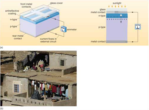
Silicon doped with boron is left with unfilled electron shells, since boron has three outer electrons, leaving the boron-doped silicon with a slight positive charge; this is a p-type semiconductor that is able to accept electrons. Layering together both n- and p-type semiconductors in wafers (Figure 5a) enhances the PV effect. Negatively charged electrons from the illuminated n-type cross the gap between the wafers to restore electrical equilibrium. However, despite the high electrical potential across the gap, large positively charged silicon atoms cannot cross it, and so only electrons can flow. The resulting current is conducted to its point of use through metal ribbons embedded in the PV wafer, which inevitably block some incoming photons. Silicon is highly reflective, so an antireflection coating is applied to the cell surface to maximize photon capture. Doped wafers and electrical conductors are generally mounted in a vacuum between glass sheets as solar PV cells for assembly in tiled arrays (e.g. Figure 5b).
Solar PV cells based on doped crystalline silicon have a theoretical maximum efficiency of 28%, because only a narrow range of short wavelength radiation from the Sun has the appropriate energy to displace electrons. In practice, they convert about 15% of the incoming solar energy in that wavelength range to electrical current. Crystalline silicon is durable but expensive to manufacture. Fine-grained, doped silicon formed into wafers is cheaper, but its efficiency is around 5 to 7%, and it eventually degrades. Current research centres on low-cost semiconducting materials, one promising candidate being fine-grained titanium dioxide - the white pigment used in paints, and therefore cheaply available. Combined with dyes to increase the sensitivity of TiO2 to sunlight, it has a practical PV efficiency of 7 to 12%, and degrades very slowly. Titanium dioxide occurs as a natural mineral (rutile - TiO2), concentrated in some beach sands because of its high density. Titanium dioxide embedded in thin plastic films may prove to be a much cheaper alternative to silicon cells. Research into PV materials is understandably a 'hot topic', and among novel possibilities are organic compounds that behave as PV semiconductors, and could be formed into flexible and strong solar cells.
What is the main practical problem that might inhibit the widespread deployment of solar cells? (Think of your household electricity supply.)
Direct current (DC) is produced, whereas all appliances linked to the 'mains' use alternating current (AC) generated by conventional turbines. Photovoltaic cells need DC-AC inverters to supply alternating current to the grid system (see Chapter 1.
Another drawback of photovoltaic solar power is the area needed to give a useful supply; a 1 m2 solar panel operates at an average power of about 30 W, so three are needed to light one 100 W light bulb. To put this in perspective, to supply the entire electricity needs of New York City with solar power would require solar cells covering an area of 192 km2; equivalent to about 25% of the city's area.