
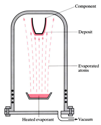
Vacuum evaporation
Variations of process include reactive evaporation (RE), activated reactive evaporation (ARE) and biased activate evaporation (BARE).
Sputtering
Variations of process include reactive sputtering, diode sputtering, high energy sputtering and magnetron sputtering.
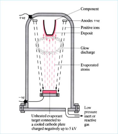
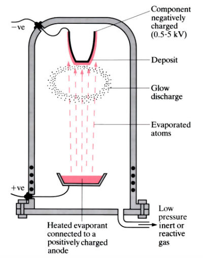
Ion plating
Variations of process include reactive ion plating (RIP), chemical ion plating (CIP) and gasless ion plating (GIP).
Manufacture:
- For vacuum evaporation and ion plating, the coating material is melted and vaporised by thermal, induction, radiation, electron beam or laser heating. In sputtering there is no melting of the material, vaporisation being achieved by bombarding solid discs, rods or cylinders of coating material with ions.
- All techniques can be used for the direct deposition of material or for “reactive” use, in which a reaction occurs in the vapour/plasma phase, between atoms of the coating material and reactive gases.
- Workpiece (substrate) temperature depends on the materials and properties required, but is typically in the range 200–400°C; considerably lower than CVD. If required, the workpiece can be heated, usually by radiant heaters.
- Processes are “line-of-sight”, necessitating rotation of the workpiece to produce even coatings, unlike CVD. The use of the sputter ion plating technique, in which the target source almost surrounds the workpiece, enables coatings to be deposited in an almost non-directional manner.
- All processes operate under vacuum; ion plating and sputtering at 0.1–1.0 Pa and vacuum evaporation at 10-5–1.0 Pa. Coverage of workpiece is usually improved as the pressure is increased.
- Cycle times depend on unit type (batch, load-lock or continuous), materials and coating thickness, but are typically in the range 1.5–3 h.
- Coating rates are less than for CVD and are typically in the range 50–500 µm h-1, depending on the technique.
- Coated components do not require any additional machining or heat treatment, although the coating costs are usually higher than for CVD. Nevertheless, costs can be as low as 1% of the finished cost of the component.
- Process can be applied to a wide variety of components, including decorative coatings on glass and plastic, corrosion resistant coatings on turbine blades and wear/corrosion resistant coatings on machine and press tools. At present the process finds its main use in the coating of twist drills, which cannot be coated by CVD due to distortion problems.
Materials:
- Almost all metals, alloys and ceramics can be coated, either directly or by the “reactive gas” technique. The sputtering process is capable of coating complex dielectrics and even some polymers.
- Single or multiple layers can be deposited, and unlike CVD the surface must be chemically clean to ensure good adhesion. Coatings usually have a low porosity.
- Despite the wide variety of materials that can be deposited, main industrial interest has centred on the coating of machine tools (particularly twist drills) and forming dies with TiN, which can give hardnesses in excess of 2000 Hv.
Design:
- Coating thickness can vary from 0.25 to 250 µm according to requirements, but is typically in the range 1–10 µm.
- Coating can be so thin that in many cases it is possible to deposit it on components within the design tolerances, thus eliminating the need for re-design.
- Due to the “line-of-sight” nature of the process, narrow, deep cavities are difficult to coat evenly.
- Process is particularly suitable for coating complex-shaped, pre-hardened steel components since the low temperatures involved do not cause softening or distortion.
- Component size depends on type of process used and the size of the coating chamber.
See Also: Ion implantation, Chemical vapour deposition (CVD), Toyota diffusion (TD), Thermal spraying, Electroplating, Electroless plating and Plasma nitriding/carburising.
This article is a part of Manupedia, a collection of information about some of the processes used to convert materials into useful objects.
Rate and Review
Rate this article
Review this article
Log into OpenLearn to leave reviews and join in the conversation.
Article reviews